
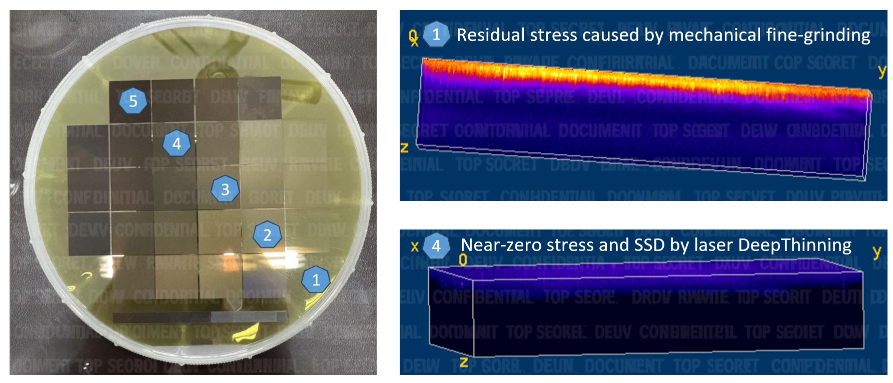
【left】 a fine-ground SiC wafer with squares treated by various laser parameters on top.
【right】SHG stress measurements of a mechanical-grinding and an optical-grinding regions, respectively.
DeepThinning (laser grinding) shows near-zero stress micromachining features.
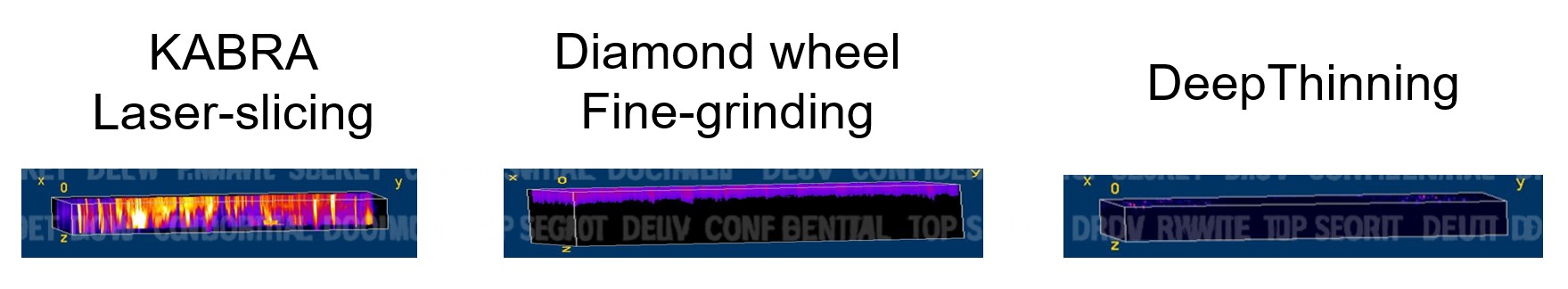
SHG stress measurements of 4H-SiC wafers after laser-slicing or fine-grinding or DeepThinning.
【right】SHG stress measurements of a mechanical-grinding and an optical-grinding regions, respectively.
DeepThinning (laser grinding) shows near-zero stress micromachining features.
SHG stress measurements of 4H-SiC wafers after laser-slicing or fine-grinding or DeepThinning.
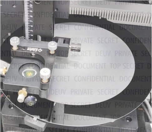
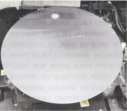
DeepThinning for a 300 mm CVD-SiC prime wafer. The removal can be controlled less than 1 µm and a removal of 1~10 µm across the whole wafer can be completed in just several minutes.
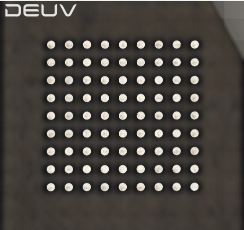
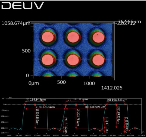
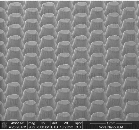
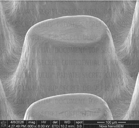
3D microstructures are fabricated on a SiC substrate by DEUV laser technology - DeepThinning.